555 Timer Schematic Symbol : 555 Timer Based Led Project Diy Electronics Projects - In the time delay mode of operation, the time is precisely controlled by one external resistor and capacitor.
byAdmin•
0
555 Timer Schematic Symbol : 555 Timer Based Led Project Diy Electronics Projects - In the time delay mode of operation, the time is precisely controlled by one external resistor and capacitor.. We need to set 555 timer in monostable mode to build timer. Nand gate conversion & example. The notations are all the same. One reduces the trigger sensitivity and the other will double the output pulse duration without increasing the values of r1 and c1. A type of variable capacitor is the trimmer capacitor that is small in size.
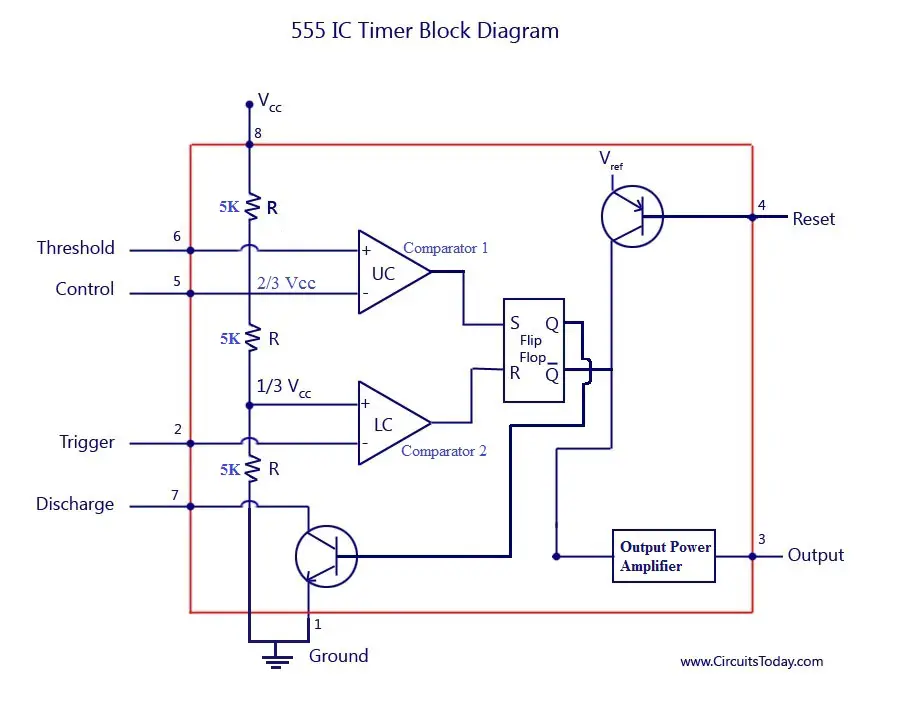
The internal block diagram and schematic of the 555 timer are highlighted with the same color across all three drawings to clarify how the chip is implemented: Between the positive supply voltage v cc and the ground gnd is a voltage divider consisting of three identical resistors, which create two reference voltages at 1 ⁄ 3 v cc and 2. We need to add a net that connects between pin 3 on our 555 timer and our r3 and r4 resistors. For a stable operation as an oscillator , the As we mentioned above, adding junctions to your schematic allows intersecting nets to share an electrical connection.
555 Timer Ic Mosquito Electronic Circuit Electronics Circuit Diagram Png 800x600px 555 Timer Ic Area Circuit from img.favpng.com Used to vary the capacitance by turning the knob. The most common use of the 555 timer is to provide timed electrical delays. They are numbered as d3, d5, d6, d9, d10, and d11. The following schematic shows two additions to the basic 555 timer circuit. T = 1.1 * r1*c1. This article covers every basic aspect of 555 timer ic. For a stable operation as an oscillator , the In monostable mode, the duration for which the pin 3 would remain high, is given by the below formulae:
The notations are all the same.
The following schematic shows two additions to the basic 555 timer circuit. Nand gate schematic of above function is given below. This will require a junction. If you look closely, you will find the '.' symbol on digital pin 3,5,6,9,10, and 11. Jan 03, 2015 · the 555 timer. The diagram below shows the actual pin arrangement of the 555 timer with the internal schematic diagram of the ic: One reduces the trigger sensitivity and the other will double the output pulse duration without increasing the values of r1 and c1. T = 1.1 * r1*c1. In monostable mode, the duration for which the pin 3 would remain high, is given by the below formulae: Jul 14, 2015 · all we need to change the value of resistor r1 and/or capacitor c1. The internal block diagram and schematic of the 555 timer are highlighted with the same color across all three drawings to clarify how the chip is implemented: Between the positive supply voltage v cc and the ground gnd is a voltage divider consisting of three identical resistors, which create two reference voltages at 1 ⁄ 3 v cc and 2. The most common use of the 555 timer is to provide timed electrical delays.
This will require a junction. Capacitor can be used in a timer circuit by adding a resistor. We need to set 555 timer in monostable mode to build timer. In the time delay mode of operation, the time is precisely controlled by one external resistor and capacitor. To add a junction, you can do it in one of two ways:
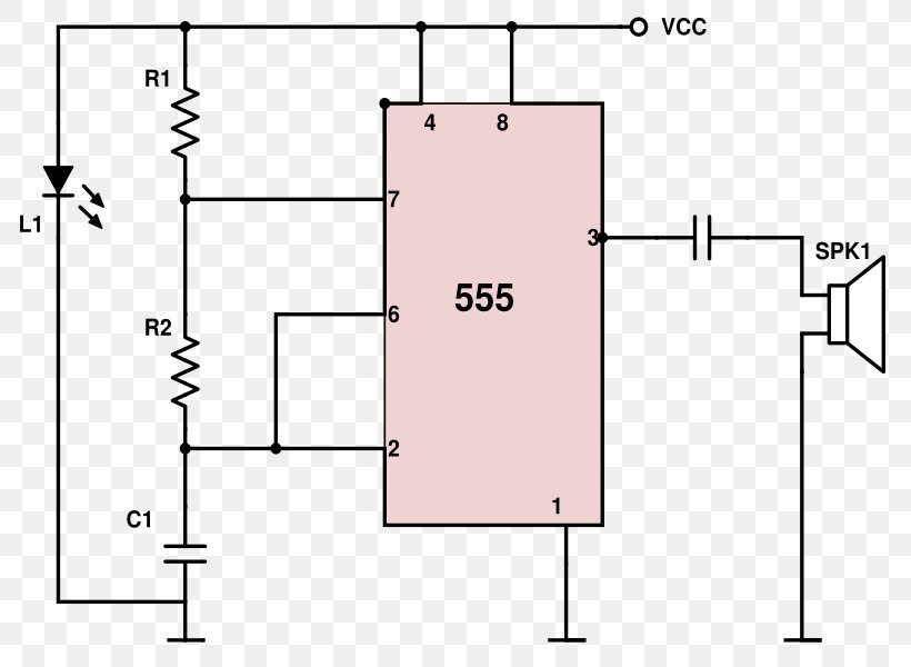
Astable Multivibrator Using 555 Timer from www.circuitstoday.com The most common use of the 555 timer is to provide timed electrical delays. To add a junction, you can do it in one of two ways: There are six pins from the set of digital pins that are pwm (pulse width modulation) pins. This will require a junction. Jan 03, 2015 · the 555 timer. We need to set 555 timer in monostable mode to build timer. They are numbered as d3, d5, d6, d9, d10, and d11. Nand gate conversion & example.
You may already know that se/ne 555 is a timer ic introduced by signetics corporation in 1970's.
This article covers every basic aspect of 555 timer ic. A type of variable capacitor is the trimmer capacitor that is small in size. Jul 14, 2015 · all we need to change the value of resistor r1 and/or capacitor c1. Nand gate conversion & example. T = 1.1 * r1*c1. The diagram below shows the actual pin arrangement of the 555 timer with the internal schematic diagram of the ic: The following schematic shows two additions to the basic 555 timer circuit. Capacitor can be used in a timer circuit by adding a resistor. In the time delay mode of operation, the time is precisely controlled by one external resistor and capacitor. If you look closely, you will find the '.' symbol on digital pin 3,5,6,9,10, and 11. In this article, we cover the following information about 555 timer ic. There are six pins from the set of digital pins that are pwm (pulse width modulation) pins. To add a junction, you can do it in one of two ways:
The most common use of the 555 timer is to provide timed electrical delays. This will require a junction. This article covers every basic aspect of 555 timer ic. Jan 03, 2015 · the 555 timer. Capacitor can be used in a timer circuit by adding a resistor.
24v Flasher Circuit Diagram Using 555 Timer Electrical Technology from www.electricaltechnology.org The diagram below shows the actual pin arrangement of the 555 timer with the internal schematic diagram of the ic: One reduces the trigger sensitivity and the other will double the output pulse duration without increasing the values of r1 and c1. There are six pins from the set of digital pins that are pwm (pulse width modulation) pins. They are numbered as d3, d5, d6, d9, d10, and d11. A type of variable capacitor is the trimmer capacitor that is small in size. T = 1.1 * r1*c1. We need to add a net that connects between pin 3 on our 555 timer and our r3 and r4 resistors. If you look closely, you will find the '.' symbol on digital pin 3,5,6,9,10, and 11.
In the time delay mode of operation, the time is precisely controlled by one external resistor and capacitor.
Between the positive supply voltage v cc and the ground gnd is a voltage divider consisting of three identical resistors, which create two reference voltages at 1 ⁄ 3 v cc and 2. The notations are all the same. Nand gate conversion & example. One reduces the trigger sensitivity and the other will double the output pulse duration without increasing the values of r1 and c1. So to build 1 minute (60 seconds) timer we need resistor of value 55k ohm and capacitor of 1000uf: We need to add a net that connects between pin 3 on our 555 timer and our r3 and r4 resistors. In the time delay mode of operation, the time is precisely controlled by one external resistor and capacitor. For a stable operation as an oscillator , the Capacitor can be used in a timer circuit by adding a resistor. They are numbered as d3, d5, d6, d9, d10, and d11. Jan 03, 2015 · the 555 timer. The most common use of the 555 timer is to provide timed electrical delays. This article covers every basic aspect of 555 timer ic.
We need to set 555 timer in monostable mode to build timer 555 timer schematic. Nand gate conversion & example.